Platinum thin film temperature resistance elements
Laser Trimming versus Sputter Etching
For many years the majority of platinum resistance thermometers were manufactured via wire wound technology (the temperature sensitive parts of the resistance elements were thin platinum wires). This process was of course very labor intensive. In addition, customer requirements were increasingly directed towards smaller physical dimensions and higher resistance values.
In order to accommodate this, the resistance wires would have to become significantly thinner. The handling and availability of such wires limited the further development of wire wound platinum resistance elements. As a result, a new manufacturing technology now known as 'thin film' was introduced approximately 25 years ago.
In this process the standard measuring wire was replaced by thin layers of platinum. These thin platinum films (thickness 1 to 2 µ ) are deposited on a flat substrate composed of AL²O³. Although cathode vaporizing proved to be the best processing method, more R&D work was necessary in order to comply with the international industrial standards DIN EN 60751.
In order to produce a defined resistance value within a small area on a thin platinum film, you need to establish a pattern on the layer. This can be achieved by the defined removal of platinum. The result is a meander shaped structure.
Laser Trimming versus Sputter Etching
Sputter etching allows for simultaneous structuring of all resistance elements on a large substrate. This method allows for a mass production process vs. the complexity of individual structuring.
Laser trimming, however, is an individual structuring process. Consequently, sputter etching is the preferred method for resistance elements of higher ohmic values (e.g. 500Ω and 1000Ω). Due to the larger meander structure of these elements, the laser trimming process requires significantly longer machining time.
Laser trimming, however, allows for a higher degree of flexibility because modifications can be made on short notice. The developments of new structures and custom designs are well suited for laser trimming technology. In addition, smaller production lots can be produced at lower cost.
Sections Three and Four provide details on the specific production techniques for each method.
Description of the Laser Trimming Process
A light beam of high energy density is produced by the use of a solid state laser. The capacity is released by using short bursts or shots. The laser beam is focused on an area of approximately 20 µ diameter using an optical device. The time and the local concentration of the capacity, in the focus, is extremely high. During this period the platinum vapors begin to liquefy in the area of the laser burst. This is similar to a combustion but without reaching a liquid state.
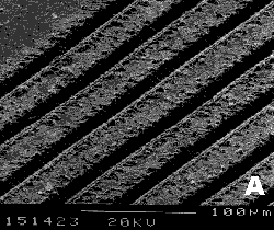 The continuous isolation cut is achieved by a precise lateral motion of the laser beam focus with a pre-defined speed for the predefined overlap of the laser burst. Photograph A shows this system of insulation cuts and the resulting meanders with a width of 15 µ.
To produce the meander shaped resistance pattern with a defined resistance value, using separation cuts against neighboring resistance elements as well as the structuring of the connection areas for the electrical contacts, requires a complicated path for the laser beam. A special motion system controlled by a programmable processor is used. The entire resistance structure is explained in Section Five.
Description of the Photolithographic Sputter Etching Process
The etching method has been designed as an alternative to the laser trimming process. This involves removing the platinum during structuring through a selective etching process.
The main steps are as follows:
a) A photosensitive lacquer of several µ thickness is deposited on the platinum coated substrate.
b) The photo lacquer is exposed through a glass mask, which already carries a metallized meander structure, which would then be depicted on the platinum layer.
c) The exposed areas are then removed using a process specific spray developer. The remaining lacquer is hardened by an annealing step. This lacquer structure is geometrically shaped precisely depicting the structure design on the platinum layer.
d) Sputter etching in a vacuum device (e.g. removal by ion bombardment). In this process the exposed platinum is etched down to the substrate. The lacquer is simultaneously removed in the same ratio as the platinum. All that remains on the substrate is the platinum structure under the lacquer layer. Once the lacquer layer is removed, (the lacquer stripping process) you arrive at the final structuring of the (untrimmed) resistance.
Laser Structured versus Sputter Etched
Resistance Elements of the Same Type
Photograph B shows a meander structure produced through the laser trimming process (magnified 500 times). Photograph C shows an equivalent system produced by the sputter etching process.
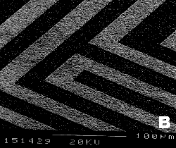 Note that the side areas of the meander originating from the laser trimming process appear to be wave shaped and less defined and show molten residue, and elevated rims due to the transition between vaporizing and heated platinum area. This by no means diminishes the quality of the laser trimmed resistance nor are there any negative effects on the long term stability or the insulation resistance between the meander lines.
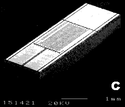 Photographs C and D show structures made by the two different processes. These samples, however, do not have connecting leads or the protective glaze.
The laser trimmed element is shown in photograph C. Look at the lower third of the photograph at the meander with the short fine trim cut at the upper left end. The majority of the total area is absorbed by the contact areas on which the connecting leads are welded at a later stage. The contact areas reach from the upper left and right to the edge of the chip limited by a laser cut. Both contact areas are separated by a double insulation laser cut.
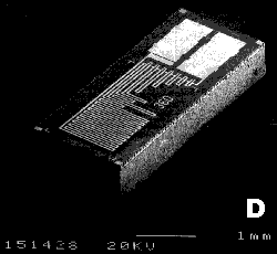 Photograph D shows a sputter etched version. In the lower third of the photo you will recognize the structure of the resistance pattern. It is comprised of a vertical main meander and seven additional 'trim loops' which can be activated by laser cutting.
In photograph E you can see loop 1, 5 and 7 next to the step shaped digital trim. There is an additional continuous fine trim through a laser cut in a closed area of the platinum layer (center picture, left half). From the picture you can see that all excessive platinum areas are removed, especially between the contact areas and the rim of the chip.
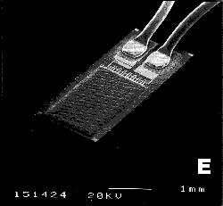 This improves electrical resistance stability, especially in the border area. On the other hand, the available area for wire contact is significantly reduced.
In order to improve the adhesion stability of the weld, all contact areas are equipped with an additional bonding pad. The lateral dimensions of the rectangular glass ceramic insulation layer, covering the meander by means of screen printing, is significantly reduced. The border areas of the chip remain metal free.

GEKON Trading GmbH
John-F-Kennedy-Str. 88 - D-63457 Hanau
+49 (0) 6181 956-270 -
